|
|
|
|
Esd electron mig sr f/f`; finger style structures. complementary circuits
Trip Point:
The voltage level of a particular signal, indicated as a fraction of Vdd, crossing which is considered as attaining logic level 1 or 0 by the signal.
Common choices are 0.5 or 0.65 or 0.9 times of vdd for level 1 and 0.35 or 0.1 times of Vdd for level 0.
Some vendors use different trip points for the input and output waveforms (especially in I/O cells).
Trip point=50% or 0.5
Transistor Matching
Transistor Matching: Connection of two transistors so that maximum power is transferred between the two. Two identical transistors, which are supposed to be the replica of each other, must have the same characteristics.
The threshold voltage and the power supply of the two similar devices should match.
If transistors are matched, it means that they are identical in all their characteristics. For matched transistors current should run in same direction. Matching of individual devices is of paramount concern in analog circuit design. In fact almost all of the 'analog layout techniques' are actually methods for improving matching between different devices on a chip. Matching is important because most analog circuit designs use a ratio based design technique (e.g. current mirrors).Some common techniques that help improve device mathcing are MULTI-GATE FINGER LAYOUT and COMMON-CENTROID LAYOUT.
MULTI-GATE FINGER LAYOUT refers to implementing a single, wide transistor as several narrow transistors in parallel. This minimizes the gate resistance and it also makes it easier to match the transistor with other devices. When referring to a multiple gate finger device one usually uses the term 'M-factor' to refer to the number of gate fingers. Therefore an M=4 device has 4 gate fingers.
MOS transistor matching is an important design parameter in many CMOS applications. MOS transistor matching in analog CMOS applications deals with statistical device differences between pairs of identically designed and identically used transistors. In analog circuit blocks, like A/D converters, threshold voltage differences of millivolts or less can determine the performance and/or yield of a product. The Golden Rules of Matching If you follow some simple rules, you can avoid gross matching problems. If you’re trying to ratio two transistors • Use the same W and L and vary M (takes out ∆W and ∆L effects) • Use M’s that are even, preferably factors of 4 (transistors are not truly symmetrical!) • Use common-centroid, or nearly common-centroid, layout (takes out oxide and doping gradients) • Use dummy transistors at the ends of the row (takes out poly etch loading and mask misalignment effects) • Make clean and well balanced routing • Use a suitable area and overdrive • Use plenty of substrate and well taps • Route currents a long way, not voltages - IR drops can cause big Mismatches Common-Centroid COMMON-CENTROID LAYOUT refers to a layout style in which a set of devices has a common center point. This is used to minimize the effect of linear process gradients (e.g. oxide thickness) in a circuit.
Q1 and Q2 have a common centroid which makes them immune from cross-chip gradients Common centroid geometry is used to reduce the offset voltage.
The technique of introducing more degrees of freedom for placement by splitting each transistor in half (same length and half width) and connecting the corresponding parts in parallel is from the common-centroid layout. Common centroid results in a circuit with twice as many transistors as the original one without altering the electrical functionality. Common centroid geometries (or point symmetric) are recommended for optimum matching. However, these structures become increasingly complex for more than two transistors, with severe penalties in area.
Static Electricity
Static electricity is defined as an electricity caused by accumulation of electric charge on the surface of an insulated material due to an imbalance of electrons resulted from the intentional charging or from the friction in low-humidity environments, which produces an electric field that can be measured and that can influence other objects at a distance.
Example: The spark that jumps from someone's hand to a doorknob after the person has walked across a carpet.
ESD (Electro Static Discharge)
Electrostatic discharge is defined as the transfer of charge between bodies at different electrical potentials.
Electrostatic discharge can change the electrical characteristics of a semiconductor device, degrading or destroying it. Electrostatic discharge also may upset the normal operation of an electronic system, causing equipment malfunction or failure. Another problem caused by static electricity occurs in clean rooms. Charged surfaces can attract and hold contaminants, making removal from the environment difficult. When attracted to the surface of a silicon wafer or a device's electrical circuitry, these particulates can cause random wafer defects and reduce product yields. ** Controlling electrostatic discharge begins with understanding how electrostatic charge occurs in the first place. Electrostatic charge is most commonly created by the contact and separation of two materials. For example, a person walking across the floor generates static electricity as shoe soles contact and then separate from the floor surface. An electronic device sliding into or out of a bag, magazine or tube generates an electrostatic charge as the device's housing and metal leads make multiple contacts and separations with the surface of the container. While the magnitude of electrostatic charge may be different in these examples, static electricity is indeed generated.
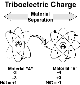
Figure 1 The Triboelectric Charge. Materials Make Intimate Contact **
Figure 2 The Triboelectric Charge - Separation
Creating electrostatic charge by contact and separation of materials is known as "triboelectric charging." It involves the transfer of electrons between materials. The atoms of a material with no static charge have an equal number of positive (+) protons in their nucleus and negative (-) electrons orbiting the nucleus. In Figure 1, Material "A" consists of atoms with equal numbers of protons and electrons. Material B also consists of atoms with equal (though perhaps different) numbers of protons and electrons. Both materials are electrically neutral.
When the two materials are placed in contact and then separated, negatively charged electrons are transferred from the surface of one material to the surface of the other material. Which material loses electrons and which gains electrons will depend on the nature of the two materials. The material that loses electrons becomes positively charged, while the material that gains electrons is negatively charged. This is shown in Figure 2.
Static electricity is measured in coulombs. The charge "q" on an object is determined by the product of the capacitance of the object "C" and the voltage potential on the object (V):
q=CV
Commonly, however, we speak of the electrostatic potential on an object, which is expressed as voltage.
This process of material contact, electron transfer and separation is really a more complex mechanism than described here. The amount of charge created by triboelectric generation is affected by the area of contact, the speed of separation, relative humidity, and other factors. Once the charge is created on a material, it becomes an "electrostatic" charge (if it remains on the material). This charge may be transferred from the material, creating an electrostatic discharge, or ESD, event. Additional factors such as the resistance of the actual discharge circuit and the contact resistance at the interface between contacting surfaces also affect the actual charge that can cause damage. ****
An electrostatic discharge (ESD) is a sudden flow of electric current through a material that is normally an insulator. A large potential difference across the insulator generates a strong electric field, converting the material's atoms into ions that conduct a current.
The best known example of ESD is a lightning strike. In this case the insulator that breaks down is air, the potential difference between cloud and ground can be millions of volts, and the resulting current that flows heats the air causing an explosive release of energy.
ESD can also be caused by so-called 'static electricity' that people experience in dry weather, when small sparks fly between insulating materials such as hair and clothing.
ESD is a serious issue in electronics, because integrated circuits are made from insulating materials such as silicon, which can break down if exposed to high voltages. Manufacturers and users of integrated circuits must take precautions to avoid this problem. Such measures include appropriate packing material, the use of conducting wrist straps and foot-straps to prevent high voltages from accumulating on workers' bodies, anti-static mats to conduct harmful electric charges away from the work area, and humidity control, because in humid conditions the surface layer of moisture on most objects conducts electric charges harmlessly to earth.
For testing the susceptibility of electronic devices to ESD from human contact, a simple test circuit called the human body model (HBM) is often used. This consists of a capacitor in series with a resistor. The capacitor is charged to a specified voltage from an external source, and then discharged through the resistor into an electrical terminal of the device under test. One of the most widely used models is defined in the JEDEC 22-A114-B standard, which specifies a 100 picofarad capacitor and a 1500 ohm resistor. Other similar standards are MIL-STD-883 Method 3015, and the ESD Association's ESD STM5.1. ** Sparks (electrons) that jump from an electrically charged object to an approaching conductive object. ** **
|
|
All rights reserved with Ranjit Inc. 2005
| |||||


 quad (common centroid) structure