ACKNOWLEDGEMENT
This project is an application of what has been taken during the current semester, its focus is on the application of flip flops, that is essential in digital design. In this case we’ve come up with a traffic light as its application. Designing such isn’t an easy task for there are some errors uneasy to detect since we have to follow the design given. In line with this, we would like to express our heartfelt appreciation to the following individuals who have helped us for the progress of this group project.
Special thanks to Ms Julie Ann Halago for the knowledge in logic design she has imparted us, as well as for the traffic light design she has lend us.
To Ms. Tereseta G. Castor and all the staff of the Main Library (Central Colleges of the Philippines) for lending us some books as our reference.
To Mr. Alex Cruz for his enhanced 555 timer design that paved way for the success of our traffic light design.
To Mr. Nathaniel Cortez for lending us his AVR. To our friends and families for their undying financial and moral support as well as for their encouragement.
Most of all, to our Almighty Father for the gift of knowledge He has allowed us to borrow.
PAROKYA NI PALOMA
The term “digital” is used to represent quantities or systems that can have only certain fixed value. For instance, a simple lamp such as the one shown below.
A simple lamp such as the one shown above is an example of a digital system because the lamp can only have two states, ON and OFF. In digital computers and other electronic digital systems work with electrical signals that can have only two possible values such as 0V and +5V. Our familiar decimal number system is not directly suitable for representing numbers in digital system because it has values from zero to ten. Therefore, in digital systems we use the binary system to represent numbers because it has only two values, 0 or 1.
BINARY SYSTEMIn the binary or base 2 number system, the weight of each digit is equal to the power of two.
|
DECIMAL NUMBER |
BINARY EQUIVALENT NUMBER |
||||
| 24 | 23 | 22 | 21 | 20 | |
| 0 | 0 | 0 | 0 | 0 | 0 |
| 1 | 0 | 0 | 0 | 0 | 1 |
| 2 | 0 | 0 | 0 | 1 | 0 |
| 3 | 0 | 0 | 0 | 1 | 1 |
| 4 | 0 | 0 | 1 | 0 | 0 |
| 5 | 0 | 0 | 1 | 0 | 1 |
| 6 | 0 | 0 | 1 | 1 | 0 |
| 7 | 0 | 0 | 1 | 1 | 1 |
| 8 | 0 | 1 | 0 | 0 | 0 |
| 9 | 0 | 1 | 0 | 0 | 1 |
| 10 | 0 | 1 | 0 | 1 | 0 |
| 11 | 0 | 1 | 0 | 1 | 1 |
| 12 | 0 | 1 | 1 | 0 | 0 |
| 13 | 0 | 1 | 1 | 0 | 1 |
| 14 | 0 | 1 | 1 | 1 | 0 |
| 15 | 0 | 1 | 1 | 1 | 1 |
| 16 | 1 | 0 | 0 | 0 | 0 |
| 17 | 1 | 0 | 0 | 0 | 1 |
| 18 | 1 | 0 | 0 | 1 | 0 |
| 19 | 1 | 0 | 0 | 1 | 1 |
| 20 | 1 | 0 | 1 | 0 | 0 |
The first digit to the left of the binary point represents 2 to the 0 power (20), which has a weight of 1. The next digit to the left of the binary point represents 22, or 4. Since each digit is just 2 times the digit to its right. The first digit to the left of the binary point represents 2 to the 0 power (20), which has a weight of 1. The next digit to the left of the binary point represents 21, which has a weight of 2. The next binary digit represents 22, or 4. since each digit is just 2 times the digit to its right. You can extend the example to as many digits as you want. For your reference, the example shows the values of powers of 2 from 2-3 to 28 . Now, lets see how you count in binary.

As we have said, digital circuitry is represents numbers and other data in binary-coded form because binary codes require only two values, such as 0 and 1. Several different terms commonly used to refer to these two values, or logic states as they are called, are:
HIGH LOW 1 0 TRUE FALSE + 5V 0 V ON OFFThe operation of some circuits is best described in terms of 1 and 0, and the operation of other circuits is best described in terms of high and low. Still others are described in terms of ON and OFF. Example of this logic gates are AND, OR, NOR, NAND, XOR, XNOR, and NOT gates (AND shall be discussed in the component used).
The figure below shows how the simplest type of latch circuit can be constructed with NAND gates. The circuit is shown with both types of NAND gates symbols, so you can use whichever one you are most comfortable with to analyze the circuit. Before we analyze the circuit, however, we need to introduce you to some labeling conventions commonly used with latches and flip-flops.
Latches and flip-flops usually have an active high output and an active low output. The active high output is identified with a Q, and the active low output is identified with a Q in figure 8-6a.
When the Q output of a latch or a flip-flop is high, the device is said to be in the set state, or just set. If the Q output is high, the Q output will. By definition, be low. When the Q output of latch or flip-flop is low, the device is said to be in the reset state, or just reset. If the Q output is low, then the Q output will, by definition, be high.
An input which directly causes a latch or flip-flop to go to the set state is labeled with an S or an S, depending on whether the input is active low or active high. Other labels commonly used to identify the set input of a device are PRESET, or just PRE.
To start, let’s predict the effect of putting a 0 on the S input and a 1 on the R input. A low on the S input causes the output to be high. The high from the Q output and the high on the R input will produce a low on the Q output of the lower NAND gate. The low on Q is fed back into one input of the upper NAND gate. If the Q output were not already high, this low would cause it to go high. With the S input low and the R input high, the circuit is in the set state. Now, lets see what happens if S is made high and R is made low.
A low on the R input causes the Q output to go high. This high, combined with the high on the S input, causes the Q output to go low. As shown by the truth table in the figure 8-6b, a low on T and a high on the S causes the circuit to go to the reset condition. The next case to consider is that where both S and R are made low. Based on the truth table for a NAND gate, S being low will cause Q to be high and R being low will cause Q to be high. This does not harm the devices, but it violates the definition of Q and Q being the complement of each other. Therefore, this input combination is referred to as indeterminate, prohibited, or invalid. This state is shown by using * in the truth table. In applications where we use this circuit, we try to make sure the input signals can never both go low at the same time.
Finally, let’s predict the effect of making both S and R high at the same time. This case is a little more difficult, because the output state depends on the logic levels that were present on S and R before they both went high. As a first example, suppose that initially the S input is low the R input is high, These input conditions will cause the Q output to be high and the Q output to be low. The low from the Q output is fed back to one input of the upper NAND gate. This low from Q will cause the Q output to be high, regardless of the logic levels on the S input. If the R input is kept high and the S input is made high, then the outputs will stay the same as they were before S was made high. A similar result occurs if the circuit is reset before S and R are both made high.If S high and R is low, then the Q output will be low and the Q output will be high. The low fed from the Q output to one input of the lower NAND gate will hold the output of this NAND gate high, regardless of the level on R input. Therefore, when R is made high, the circuit just remains in the reset state.
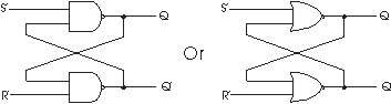
Fig 8-6b

Miniature Aluminum Radial Electrolytic Capacitors


Fixed Resistor
Potentiometer (Variable Resistor).